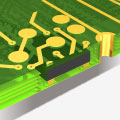
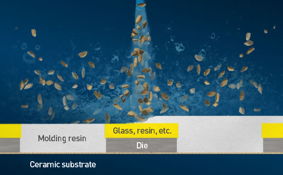
Removal of overmolding from embedded LED chips
Processing Details
- Scraping
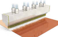
Fine surface processing of LED package with wet blasting
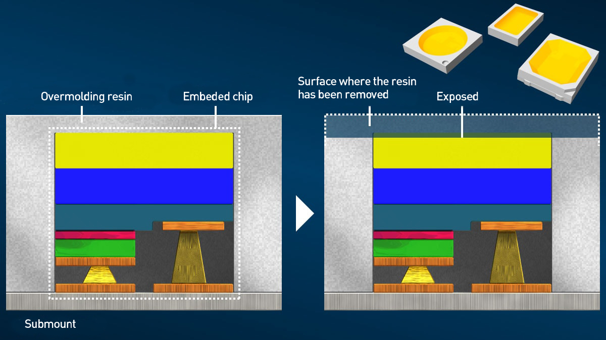
This treatment scrapes the overmolding resin (white resin/sealing resin/reflector resin) such as epoxy or silicone on the LED device that covers the chips as a result of LED device manufacturing in order to expose the chips and electrodes. During mass production of small LED devices, the chips are exposed minimizing damage.
It is effective for manufacturing of flip and chip on board (COB) chip LEDs, and can be used to expose chips buried during resin molding.
Wet Blasting Characteristics
- Fine particles are used to minimize damage to the chips and electrodes.
- Easy to control the processing rate by changing the operating air pressure and number of passes.
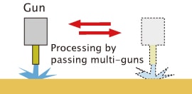
- The processing time is short because multiple targets can be processed at once.
Processing Image
Advantages of wet blasting: Controllability
The abrasive material is mixed with water and treated as a fluid, so the processing rate is highly controllable and it is easy to set the processing strength as required.
Processing Condition
| Abrasive Used | Alumina A#2000 |
|---|---|
| Air Pressure | 0.25 MPa |
| Processing Speed | 20 mm/sec |
| Projectiion (Spray) Angle | 90° |
| Number of Passes for Processing | 4-10 passes |
Difference in processing rate between filler-containing resin and copper.
Possible to control the processing rate by changing the abrasive type and air pressure.
 Untreated
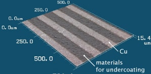 After 4 passes: Step 0 µm
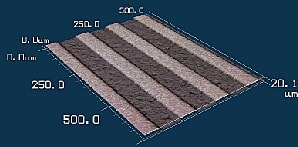 After 6 passes: Step 7 µm
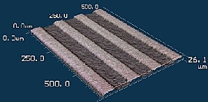 After 8 passes: Step 14 µm
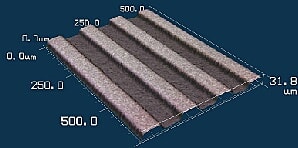 After 10 passes: Step 20 µm
※The amount of Copper being shaved is 0.2 µm.